- 您现在的位置:买卖IC网 > Sheet目录407 > DMN6068LK3-13 (Diodes Inc)MOSFET N-CH 60V 6A DPAK
�� �
�
�DMN6068LK3�
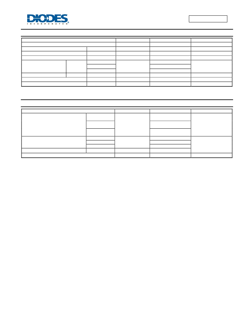
�Maximum� Ratings�
�(@T� A� =� +25°C,� unless� otherwise� specified.)�
�Drain-Source� voltage�
�Characteristic�
�Symbol�
�V� DSS�
�Value�
�60�
�Unit�
�V�
�Gate-Source� voltage�
�Single� Pulsed� Avalanche� Energy�
�Single� Pulsed� Avalanche� Current�
�(Note� 5)�
�(Note� 11)�
�(Note� 11)�
�V� GS�
�E� AS�
�I� AS�
�±� 20�
�37.5�
�5.0�
�V�
�mJ�
�A�
�(Note� 7)�
�8.5�
�Continuous� Drain� current�
�V� GS� =� 10V�
�T� A� = 70� °� C (Note 7)�
�I� D�
�6.8�
�A�
�(Note� 6)�
�6.0�
�Pulsed� Drain� current�
�V� GS� =� 10V�
�(Note� 8)�
�I� DM�
�22.2�
�A�
�Continuous� Source� current� (Body� diode)�
�Pulsed� Source� current� (Body� diode)�
�(Note� 7)�
�(Note� 8)�
�I� S�
�I� SM�
�10.2�
�22.2�
�A�
�A�
�Thermal� Characteristics� (@T� A� =� +25°C,� unless� otherwise� specified.)�
�Characteristic�
�(Note� 6)�
�Symbol�
�Value�
�4.12�
�33�
�Unit�
�Power� dissipation�
�Linear� derating� factor�
�(Note� 7)�
�P� D�
�8.49�
�67.9�
�W�
�mW/� °� C�
�(Note� 9)�
�(Note� 6)�
�2.12�
�16.9�
�30.3�
�Thermal� Resistance,� Junction� to� Ambient�
�Thermal� Resistance,� Junction� to� Lead�
�Operating� and� storage� temperature� range�
�(Note� 7)�
�(Note� 9)�
�(Note� 10)�
�R� θ� JA�
�R� θ� JL�
�T� J� ,� T� STG�
�14.7�
�59.0�
�3.09�
�-55� to� +150�
�°� C/W�
�°� C�
�Notes:�
�5.� AEC-Q101� V� GS� maximum� is� ±16V.�
�6.� For� a� device� surface� mounted� on� 50mm� x� 50mm� x� 1.6mm� FR4� PCB� with� high� coverage� of� single� sided� 2oz� copper,� in� still� air� conditions;� the� device� is�
�measured� when� operating� in� a� steady-state� condition.�
�7.� Same� as� note� 2,� except� the� device� is� measured� at� t� ≤� 10� sec.�
�8.� Same� as� note� 2,� except� the� device� is� pulsed� with� D� =� 0.02� and� pulse� width� 300� μs.� The� pulse� current� is� limited� by� the� maximum� junction� temperature.�
�9.� For� a� device� surface� mounted� on� 25mm� x� 25mm� x� 1.6mm� FR4� PCB� with� high� coverage� of� single� sided� 1oz� copper,� in� still� air� conditions;� the� device� is�
�measured� when� operating� in� a� steady-state� condition.�
�10.� Thermal� resistance� from� junction� to� solder-point� (at� the� end� of� the� drain� lead).�
�11.� UIS� in� production� with� L� =� 3.0mH,� I� AS� =� 5.0A,� R� G� =� 25?� ,� V� DD� =� 50V,� starting� T� J� =� 25°C�
�DMN6068LK3�
�Document� Number� DS32057� Rev� 4� -� 2�
�2� of� 8�
�www.diodes.com�
�May� 2013�
�?� Diodes� Incorporated�
�发布紧急采购,3分钟左右您将得到回复。
相关PDF资料
DMN6068SE-13
MOSFET N-CH 60V 4.1A SOT223
DMN62D0LFB-7B
MOSFET N-CH 60V 100MA 3-DFN
DMN62D0SFD-7
MOSFET N-CH 60V 540MA 3-DFN
DMN65D8LDW-7
MOSF N CH DUAL 60V 180MA SOT363
DMN65D8LFB-7B
MOSF N CH 60V 260MA X1-DFN1006-3
DMN65D8LW-7
MOSFET N CH 60V 300MA SOT323
DMN66D0LDW-7
MOSFET N-CH DUAL 115MA SOT-363
DMN66D0LT-7
MOSFET N-CH 60V 115MA SOT-523
相关代理商/技术参数
DMN6068SE
制造商:Diodes Incorporated 功能描述:MOSFET N CH DIOD 60V 4.1A SOT223 制造商:Diodes Incorporated 功能描述:MOSFET, N CH, DIOD, 60V, 4.1A, SOT223 制造商:Diodes Incorporated 功能描述:MOSFET, N CH, DIOD, 60V, 4.1A, SOT223, Transistor Polarity:N Channel, Continuous
DMN6068SE_11
制造商:DIODES 制造商全称:Diodes Incorporated 功能描述:60V N-CHANNEL ENHANCEMENT MODE MOSFET
DMN6068SE-13
功能描述:MOSFET ENHANCE MODE MOSFET 60V N-CHAN RoHS:否 制造商:STMicroelectronics 晶体管极性:N-Channel 汲极/源极击穿电压:650 V 闸/源击穿电压:25 V 漏极连续电流:130 A 电阻汲极/源极 RDS(导通):0.014 Ohms 配置:Single 最大工作温度: 安装风格:Through Hole 封装 / 箱体:Max247 封装:Tube
DMN62D0LFB
制造商:DIODES 制造商全称:Diodes Incorporated 功能描述:N-CHANNEL ENHANCEMENT MODE MOSFET
DMN62D0LFB-7
功能描述:MOSFET MOSFET BVDSS: 41V-60 X2-DFN1006-3 T&R 3K RoHS:否 制造商:STMicroelectronics 晶体管极性:N-Channel 汲极/源极击穿电压:650 V 闸/源击穿电压:25 V 漏极连续电流:130 A 电阻汲极/源极 RDS(导通):0.014 Ohms 配置:Single 最大工作温度: 安装风格:Through Hole 封装 / 箱体:Max247 封装:Tube
DMN62D0LFB-7B
功能描述:MOSFET N-CH 60V 100MA 3-DFN RoHS:是 类别:分离式半导体产品 >> FET - 单 系列:- 标准包装:1,000 系列:MESH OVERLAY™ FET 型:MOSFET N 通道,金属氧化物 FET 特点:逻辑电平门 漏极至源极电压(Vdss):200V 电流 - 连续漏极(Id) @ 25° C:18A 开态Rds(最大)@ Id, Vgs @ 25° C:180 毫欧 @ 9A,10V Id 时的 Vgs(th)(最大):4V @ 250µA 闸电荷(Qg) @ Vgs:72nC @ 10V 输入电容 (Ciss) @ Vds:1560pF @ 25V 功率 - 最大:40W 安装类型:通孔 封装/外壳:TO-220-3 整包 供应商设备封装:TO-220FP 包装:管件
DMN62D0SFD-7
功能描述:两极晶体管 - BJT MOSFET BVDSS RoHS:否 制造商:STMicroelectronics 配置: 晶体管极性:PNP 集电极—基极电压 VCBO: 集电极—发射极最大电压 VCEO:- 40 V 发射极 - 基极电压 VEBO:- 6 V 集电极—射极饱和电压: 最大直流电集电极电流: 增益带宽产品fT: 直流集电极/Base Gain hfe Min:100 A 最大工作温度: 安装风格:SMD/SMT 封装 / 箱体:PowerFLAT 2 x 2
DMN62D1SFB-7B
功能描述:MOSFET MOSFET BVDSS RoHS:否 制造商:STMicroelectronics 晶体管极性:N-Channel 汲极/源极击穿电压:650 V 闸/源击穿电压:25 V 漏极连续电流:130 A 电阻汲极/源极 RDS(导通):0.014 Ohms 配置:Single 最大工作温度: 安装风格:Through Hole 封装 / 箱体:Max247 封装:Tube